
Credit: Image courtesy of Feng Wang, Berkeley Lab
Berkeley Lab researchers use light to dope graphene boron nitride heterostructures
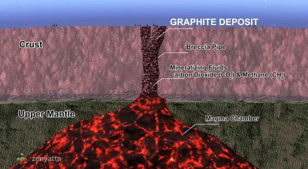
THUNDER BAY – The Ring of Fire in Northern Ontario and its chromite potential might be the top focus for many in the region. However it is very likely in the longer run, the “Arc of Fire” which includes graphite could end up having the greatest long term impact on our society.
The Zenyatta Albany Project near the Constance Lake First Nation along with development and exploration of several other nearby projects has generated small excitement over recent years.
Zenyatta Ventures
The majority of the world’s supply of graphite, a major component in graphene as been in Sri Lanka and Asia. The potential of a major vein graphite source in Canada could shift the scale in the world of graphite.
Why is this a big deal?
Graphene continues to reign as the next potential superstar material for the electronics industry, a slimmer, stronger and much faster electron conductor than silicon.
With no natural energy band-gap, however, graphene’s superfast conductance can’t be switched off, a serious drawback for transistors and other electronic devices.
Various techniques have been deployed to overcome this problem with one of the most promising being the integration of ultrathin layers of graphene and boron nitride into two-dimensional heterostructures.
As conductors, these bilayered hybrids are almost as fast as pure graphene, plus they are well-suited for making devices. However, tailoring the electronic properties of graphene boron nitride (GBN) heterostructures has been a tricky affair, involving chemical doping or electrostatic-gating – until now.
Researchers with Berkeley Lab and the University of California (UC) Berkeley have demonstrated a technique whereby the electronic properties of GBN heterostructures can be modified with visible light. Feng Wang, a condensed matter physicist with Berkeley Lab’s Materials Sciences Division and UC Berkeley’s Physics Department, as well as an investigator for the Kavli Energy NanoSciences Institute at Berkeley, led a study in which photo-induced doping of GBN heterostructures was used to create p–n junctions and other useful doping profiles while preserving the material’s remarkably high electron mobility.
“We’ve demonstrated that visible light can induce a robust writing and erasing of charge-doping in GBN heterostructures without sacrificing high carrier mobility,” Wang says. “The use of visible light gives us incredible flexibility and, unlike electrostatic gating and chemical doping, does not require multi-step fabrication processes that reduce sample quality. Additionally, different patterns can be imparted and erased at will, which was not possible with doping techniques previously used on GBN heterostructures.”
Graphene is a single layer of carbon atoms arranged in a hexagonal lattice. Boron nitride is a layered compound that features a similar hexagonal lattice – in fact hexagonal boron nitride is sometimes referred to as “white graphene.” Bound together by the relatively weak intermolecular attraction known as the van der Waals force, GBN heterostructures have shown high potential to serve as platforms not only for high-electron-mobility transistors, but also for optoelectronic applications, including photodetectors and photovoltaic cells.
The key to future success will be the ability to dope these materials in a commercially scalable manner. The photo-induced modulation doping technique developed by Wang and a large team of collaborators meets this requirement as it is comparable to the photolithography schemes widely used today for mass production in the semiconductor industry. Illumination of a GBN heterostructure even with just an incandescent lamp can modify electron-transport in the graphene layer by inducing a positive-charge distribution in the boron nitride layer that becomes fixed when the illumination is turned off.
“We’ve shown show that this photo-induced doping arises from microscopically coupled optical and electrical responses in the GBN heterostructures, including optical excitation of defect transitions in boron nitride, electrical transport in graphene, and charge transfer between boron nitride and graphene,” Wang says. “This is analogous to the modulation doping first developed for high-quality semiconductors.”
While the photo-induced modulation doping of GBN heterostructures only lasted a few days if the sample was kept in darkness – further exposure to light erased the effect – this is not a concern as Wang explains.
“A few days of modulation doping are sufficient for many avenues of scientific inquiry, and for some device applications, the rewritability we can provide is needed more than long term stability,” he says. “For the moment, what we have is a simple technique for inhomogeneous doping in a high-mobility graphene material that opens the door to novel scientific studies and applications.”


